From FPD to Semiconductors — A Company That Has Always Chosen Change to Grow
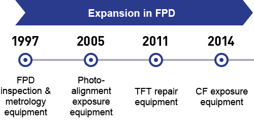
Founded in 1997 as a manufacturer of FPD inspection systems, V Technology has expanded its technological domains through both M&A and in-house development, building capabilities in photo-alignment exposure systems, TFT repair systems, CF (color filter) exposure systems, and more.
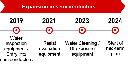
As the smartphone and television markets matured, however, growth in the FPD market slowed after peaking in 2019. It was then that we made the decision to take on the semiconductor market as a new arena for growth.
This shift was driven by more than simply "being able to do it technically." With expanding demand from AI, autonomous driving, and data centers, the semiconductor market is an area expected to keep growing—making it, from a management standpoint, a market we should enter.
Our Evolution
The Same Core Technology
Alignment of huge glass substrates
High-precision patterning /
Pixel-defect inspection
Use of optics & image processing
micron- to nano-level
“Align,” “Measure,” and “Control”
Nano-level alignment for finer geometries
Resist-pattern evaluation
Wafer-defect inspection
Application of high-resolution cameras & optics
V Technology's core technology lies in aligning, measuring, and controlling positions at the micron-to-nanometer level.
●FPD manufacturing requires high-precision patterning on enormous glass substrates
●Semiconductor manufacturing, as miniaturization advances, demands nanometer-level alignment
In other words, the essence of the technology required was the same.
It was precisely because we had this technological foundation that our expansion into semiconductor equipment proceeded so naturally.
The further semiconductor miniaturization advances, the more important the technology to "see the unseeable" becomes.
V Technology's original strengths lay in:
・High-resolution cameras
・Optical systems
・Image-processing algorithms
・Nanometer-precision measurement technology
All of these could be applied directly to semiconductor inspection and metrology systems.
A structural shift in the market and our own technology met at exactly the right moment.
Our equipment is directly connected to advances in people's lives and in social infrastructure, including:
・Sharper image quality in smartphones
・Improved safety in in-vehicle displays
・Higher performance in semiconductors for AI servers
・Greater energy efficiency in data centers
V Technology will continue to refine the technology that supports the world from places unseen.